Growth
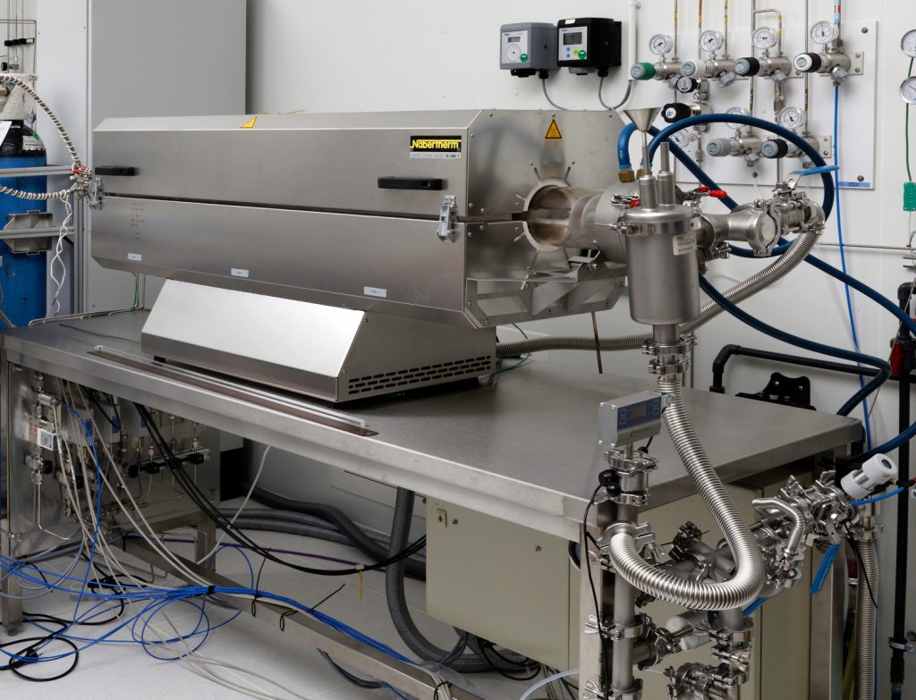
WSe2, WTe2 and ternary alloy WSeTe are synthized at C2N using Chemical Vapor Depositon (CVD). This technique allows to obtain “wide” (several tens of microns) monocrystal of controlled thickness (1, 2, 3 monolayer) after the careful optimization of the growth parameter (temperatures, pressure, gas flows). The standard substrates currently used at C2N are thermal silica (SiO2) and graphene on SiC.

The CVD growth equipement is part of the POEM platerform of the C2N technological facilities
Characterization
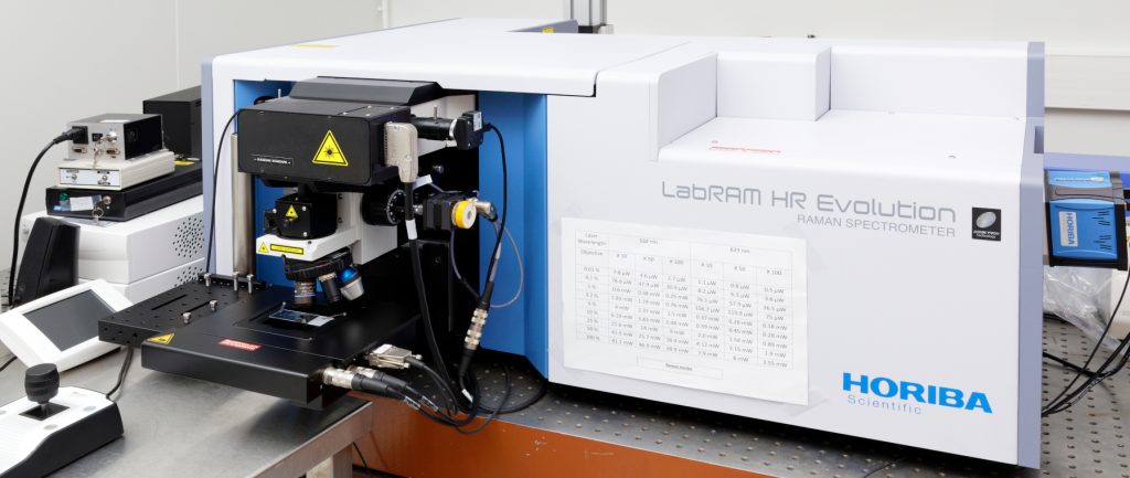
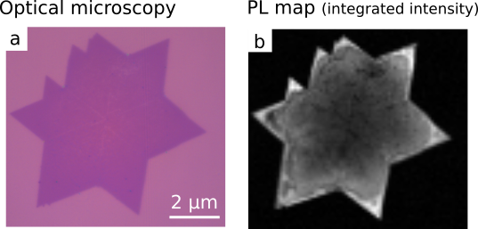
The sample are first characterized by optical microscopy, room temperature photo-luminescence (PL) and room temperature Raman spectroscopy. The PL and Raman are performed in a combined optical maper (Horiba) which allows to spatially map the PL and Raman response of selected monocrystals.


In addition to the above methods, specific tools such as Transmission Electron Microscopy (TEM, the PANAM platform, X-ray diffraction, and other tools (SEM, LEED, EDX) are available to further investigate the structure and the properties of the grown materials.
Fabrication
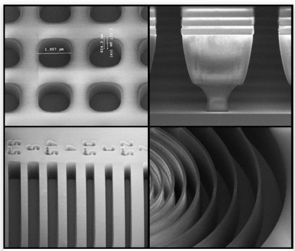
The C2N laboratory host an large clean room (the PIMENT technological platform) which cover a very wide range of micro- and nano-fabrication technique, from standard wafer processing to small research samples.

